
For years, the semiconductor world has banked its future on chiplet challenges. The promise was simple and elegant: break down massive, monolithic chips into smaller, Lego-like “chiplets” that could be mixed and matched to create powerful, custom processors more cheaply and efficiently. However, as of May 2026, that utopian vision is colliding with a harsh reality. Groundbreaking analysis from sources like Semiconductor Engineering confirms that the transition to the technology is proving far more difficult than anticipated.
Table of Contents
The core issues are no longer theoretical. The industry is grappling with escalating packaging costs, confusing and sometimes conflicting interconnect standards, and major reliability questions about the very materials used to hold these complex assemblies together. This isn’t just a minor setback; it’s a systemic engineering and economic challenge that questions the foundational assumptions behind the this innovation revolution.
The Fractured State of chiplet challenges
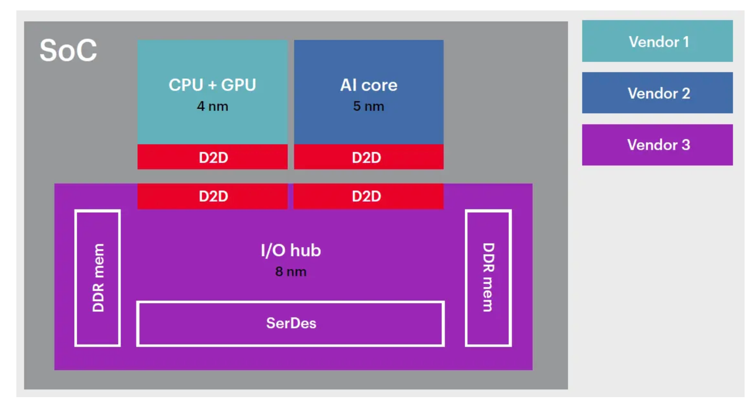
To grasp the present situation, one must first map the battlefield. The world of the system is not a single, unified front but a collection of competing empires. Tech giants like Intel and AMD have been the most visible proponents, using chiplet designs to push the performance of their server and desktop CPUs. AMD, in particular, found massive success by leveraging it to compete with Intel, using chiplets manufactured by TSMC.
The true control often lies a layer deeper, with the companies that provide the “how.” TSMC’s CoWoS (Chip on Wafer on Substrate) packaging technology is a critical enabler, creating a technical moat that is extremely difficult for others to cross. This creates a dependency; you can design the best chiplet in the world, but if you can’t access the advanced packaging to connect it, your design is worthless. Even with the establishment of the Universal Chiplet Interconnect Express (UCIe) standard, which aims to create an open ecosystem, proprietary solutions and “walled gardens” persist. This division is a central source of the current challenges facing the platform.
Also read: Silicon photonics: Nvidia’s Critical $6.5B Gamble on AI’s Future
chiplet challenges: Why the Economics Are Faltering
The primary argument for the technology was economic. By manufacturing smaller dies, companies could achieve better yields and lower costs compared to producing one enormous, monolithic chip where a single defect could ruin the entire unit. On paper, this is sound. However, in reality, as detailed in recent industry analyses, is that second-order costs are spiraling out of control.
A detailed report from Semiconductor Engineering confirms that the economics are more complicated than initially believed. The expenses associated with advanced 2.5D and 3D packaging, such as creating silicon interposers and managing thermal stress, are enormous. Furthermore, the challenge of testing and validating each individual chiplet to ensure it is a “known-good-die” (KGD) before the costly final assembly adds another layer of complexity and expense that many early models underestimated.
What’s more, new reliability issues are emerging. The low-temperature solders required for some advanced packaging techniques are proving to be brittle and susceptible to failure under thermal stress, creating a long-term risk for devices that are supposed to last for years in data centers and vehicles. This combination of high upfront costs and long-term reliability risks is a dangerous cocktail that is making many question the true total cost of ownership for this innovation systems.
Regulatory and Technical Friction in chiplet challenges
At the heart of the problem is a fundamental contradiction. For the the system ecosystem to thrive, it needs a genuinely open and reliable standard that allows components from different vendors to work together seamlessly. The UCIe standard was created for this exact purpose. Ironically, the players advocating for openness also have powerful incentives to lock customers into their own proprietary, high-margin solutions.
This results in a deadlock. While UCIe has seen updates and adoption, its progress has been slower than hoped, and many of its advanced management features are optional, allowing vendors to create subtly incompatible versions. Analysts, including those from firms like Gartner, have pointed to the immense challenge of assigning liability in a multi-vendor system. When a system with chiplets from three different companies fails, who is responsible? The designer, the foundry, the packaging house, or the interconnect standard itself?
This unresolved liability is a significant business risk that chills investment and slows adoption, particularly in mission-critical sectors like automotive and aerospace where reliability is non-negotiable. Until the industry can solve the “blame game” inherent in multi-vendor it, the dream of a universal, plug-and-play ecosystem will remain just that—a dream.
You might also like: Trailing-edge foundry: A Critical Look at 2026’s Chip Wars
The Bottom Line on chiplet challenges
When all is said and done, the platform is not dead, but the initial euphoria has given way to a sobering period of engineering and economic reckoning. The transition from a monolithic design philosophy to a modular one is proving to be substantially more difficult than the early hype suggested. The promise of Lego-like simplicity has been replaced by the reality of multi-physics complexity, fractured standards, and daunting reliability hurdles. For investors, engineers, and tech strategists, ignoring these warning signs would be a costly mistake.
Critical Signals to Watch:
* Watch for: The adoption rate and, more importantly, the enforcement of mandatory compliance within the UCIe 2.0+ specifications.
* Track: Public statements from TSMC, Intel, and Samsung regarding “known-good-die” (KGD) yields and advanced packaging costs.
* Pay attention to: The first major product failure or recall publicly attributed to multi-vendor the technology reliability issues.
* An important metric: Any slowdown in hyperscaler investment in chiplet-based architectures, as noted in forecasts from firms like Gartner.
* Evaluate: The launch of any new high-performance proprietary interconnects by major players, which would signal a retreat from the open ecosystem ideal.
The future of chiplet challenges is not guaranteed. It requires a level of industry-wide collaboration on standards, testing, and reliability that has so far been elusive. The coming 18-24 months will be critical in determining whether these challenges can be overcome, or if the industry will be forced to seek a different path beyond Moore’s Law.